When was the last time you drove a car or used an appliance that didn’t include some kind of electronic component? Across industries, electronic devices are becoming commonplace in vehicles, medical devices, and home appliances. They’re also showing up in new places all the time from doorbells to bathroom fixtures.
What’s more, devices and the circuit boards that control them are getting smaller and using higher speed processors to communicate between components, transmit sensor data, and even control the equipment itself. Electromagnetic and radio frequency interference have always been a concern with electronics, but with more devices in proximity to each other and more computing power housed in each, radiation and sensitivity to emissions are more critical than ever before. And that means increased attention to electromagnetic interference (EMI) and radiofrequency interference (RFI) shielding.
In the automotive industry, PCBs are used for infotainment systems, wireless communications, sensors and cameras, for safety and semi-autonomous driving features, and more. Safety is the primary concern for automakers and their suppliers, but fuel efficiency and lightweight vehicle design are perennial priorities too. All of these concerns affect EMI/RFI shield design and manufacturing since components are so interconnected.
Causes and consequences of interference
Interference happens when one of the electromagnetic or radio frequency waves generated by one device affect another device. Just like static on an AM or FM radio, interference makes the device’s signal unclear and less likely to be correctly decoded by the receiving device. It’s annoying when interference disrupts your favorite song, but it can be deadly when it prevents your forward-collision warning system from detecting an oncoming vehicle.
To be most effective, electronic signals need to transmit completely and without “noise” from interference. One of the best ways to do this is by shielding sensitive components on circuit boards. Shielding serves two main purposes: to trap waves within a circuit and reflect them away from other circuits and to absorb or block waves emitted by nearby circuits. Note that interfering waves can be from other devices within the vehicle (or appliance or medical device) or from external sources such as cell phone towers, radio towers, and power transmission lines.
Basics of effective shielding
Precision-stamped shields are generally made of metals that are conductive and magnetically permeable. A range of materials can be used, depending on specific shielding goals including reflection, absorption, weight, and solderability. Common metals for shields include copper, brass, and steel. Coatings of tin or nickel may also be used to protect the base metals.
Another side effect of adding compact electronics to vehicles and other devices is a phenomenon known as “skin effect,” in which currents tend to concentrate in the top layers of a conductor. This has the effect of raising “current density,” which means shields need to be not only small but capable of reflecting and/or absorbing high levels of interference.
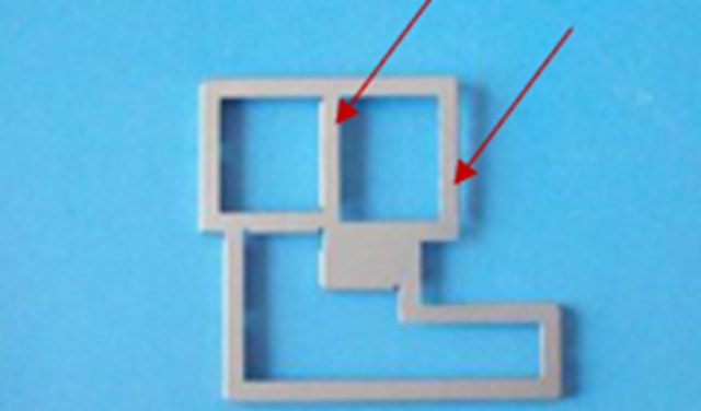
Shields are generally boxes or cages that cover individual circuits or a group, depending on the wavelengths and interference to be reflected or absorbed. Sides may be solid or may contain holes, or apertures, depending on the wavelength(s), airflow/thermal buildup considerations, and component weight needs. In most stamped component applications, shields are attached to the PCB with pins that go through the board or surface-mounted, usually by soldering.
As frequencies increase, their wavelengths shorten. This means waves are smaller and are more prone to leak out of shielding enclosures or seep into them. For example, “for a frequency of 100 GHz, the corresponding wavelength is 0.12 inches. Typically, holes should be no larger than 1/20th to 1/50th of a wavelength, and if anything, they may need to be smaller, so this calculates to 3 to 6 mil hole or aperture,” according to this guide from Interference Technology.
Working with a stamper
You’re the expert on the shielding effectiveness (SE) of the part. Because SE requirements affect part geometry and because tolerances in the shrinking world of electronics are tight, it’s helpful to share design intent details with your stamper. This ensures critical features are retained and manufacturing efficiency is optimal, without compromising SE. Tell your stamper about requirements for things like reflecting or absorbing interference, aperture size, corner design/leakage concerns, weight limits (component, device, or vehicle), shield size relative to the board or device, and environmental considerations (e.g. corrosion, vibrations).
An experienced precision stamper can help you save time and money by reviewing your design to assess manufacturability and providing feedback on things like tolerances, critical dimensions, and even optimal design for cleaning of the finished part.
For example, a customer may be advised to widen a shield’s frames as much as possible in areas that don’t affect assembly and end-use. This makes stamping and forming easier because the part is more stable with more material to hold during manufacturing. A wider frame is also stronger, with less potential for deformation in subsequent use. Best of all, the benefits of adjusting the design don’t increase the part’s cost because the gross weight of the part does not change.
Part performance is also affected by how clean it is, or its technical cleanliness. In this kind of cleaning, metallic particles, fibers, and other microscopic debris, are removed from parts with blown air, ultrasonic washing and rinsing, and heat drying. Particles can affect solderability, component fit-up, and more, so it’s important to be sure your precision stamper has the tools and knowledge to clean parts to spec. Depending on requirements, things like plating and part geometry can affect the cleaning process, so be sure to discuss these details with the stamper.
EMI shielding is critical in today’s electronics market. But creating the best possible shield is complex due to the amount and variety of frequencies surrounding circuits, and because part design affects both SE and manufacturability. If you’re looking for a stamping partner you can trust for your custom design, contact us today!

