As electronic devices play an ever-larger role in automotive, aviation, medical, other industries, the electromagnetic/radio frequency interference (EMI/RFI) shielding market continues to expand:
The global EMI Shielding market is expected to grow from USD 5.46 Billion in 2017 to USD 9.91 Billion by 2025 at a CAGR of 7.7% during the forecast period from 2018-2025.
Within the EMI shielding market, the automotive industry is expected to exhibit the highest growth from 2019 to 2024.
Devices and circuit boards are trending smaller and faster, and electromagnetic Compatibility (EMC) (EMC) requirements are strict. This means there’s a continuing need for better interference control if you hope to bring new devices and finished products to market, and custom shielding is a big part of that. Metal shields offer a trusted and durable solution to many shielding needs. But given how many electronic and communications devices are packed into many products these days, shields can’t merely be designed well, they need to be manufactured with care to minimize the risk of EMI and RFI on devices. For many OEMs and suppliers, this is where custom precision stamping comes in.
A Growing Market for EMI Shields
Electromagnetic and radiofrequency radiation and the interference they cause come from external sources, such as radio and cell phone towers, and sources within devices themselves, such as microprocessors. As 5G networks expand and vehicles and other consumer products incorporate more built-in electronics and “smart” features, there are more sources of radiation and more components vulnerable to interference-based malfunction. The result? Growing demand for custom EMI/RFI shields driven by:
5G networks. “Ongoing demonstrations of field trials and pilot projects to develop the viability of 5G technology and stringent environmental and EMC regulations across industries” mean the presence of these networks will continue to expand. Regulations to deal with their effects will also change and require more stringent shielding, notes research from Markets and Markets.
Vehicle components. Nonmetallic auto body components like bumpers and panels are non-conductive and less protective from external EMI sources. Electric drivetrains increase the number of electronic control units and sensors in a vehicle, and contribute to EMI generated as well as presenting more components that are sensitive to it.
Demand for autonomous and semi-autonomous vehicles. In all vehicles, but especially autonomous/semi-autonomous ones, protecting passengers depends on properly functioning electrical components and sensors. Shielding is one way to ensure electronics will work as intended every time. “In an autonomous car, the communications link between a LIDAR object-detection camera and the ECU responsible for control of the speed and direction of movement is as safety-critical as the hydraulic link between the brake pedal and the brakes in a non- or semi-autonomous car,” says EE News.
Standard inclusion of electronic and sensor-based features in most vehicles. “Modern cars and trucks can have up to 100 networked microprocessors running 150 million lines of code with thousands of supporting active components,” according to Electronic Design. This includes convenience features (e.g. onboard GPS navigation systems, touchscreen infotainment systems, handsfree features, Bluetooth capabilities) and safety features (e.g. terrain management systems, parking assistance, automatic emergency braking, adaptive cruise control, forward collision warning, and door entry and lock systems). All of these emit and may be affected by electromagnetic radiation-based interference and can be safeguarded with shields.
Electromagnetic radiation, interference, and what causes it
Electromagnetic (EM) radiation comes in the form of waves of alternating electric and magnetic energy. The frequency of a wave (i.e. how often a new wave is produced) is inversely related to the size of the wave: higher frequency (i.e. faster) equals smaller wavelength.
While they’re in operation, all electronic and communication devices produce radiation that falls somewhere within the range of wavelengths on the electromagnetic spectrum. Subsets of this spectrum are the radio wave and microwave ranges, which are frequently used with printable circuit boards (PCBs) as well as communication and safety devices in vehicles. Radio frequencies are used with communication devices like radios, cell phones, wifi, even power lines and signal cables within devices. They have wavelengths between 1 m and 100 km and frequencies between 300 MHz and 3 kHz. Microwaves are used for applications including radar and navigation systems, at wavelengths between 1 m and 1 mm with frequencies between 300 MHz and 300 GHz. Some applications also use Millimeter wavelengths and frequencies, which are even faster and smaller.
Medical, military, and aircraft equipment and vehicles are steadily incorporating more electronics that decrease in size, increase in speed (due to faster processors and especially higher speed digital circuits), EM frequency goes up and wavelength goes down. These smaller wavelengths are challenging to contain and reflect so they don’t cause problems in the larger device.
Internally generated radiation, which is radiation emitted from the circuit itself, can also travel along wires and cables connecting circuits and components and contribute to interference from a distance.
Interference can also be caused by cavity resonance. It occurs inside a conductive enclosure (i.e. EMI shield or “cavity”) when frequencies inside the enclosure are similar to those of the circuit. The resulting resonance creates additional interference and impacts the enclosure’s ability to effectively shield the circuit and its surroundings.
Interference comes from external sources too, such as cell phones, lightening, overhead power lines, and solar flares.
The impact of interference
Cellphones, CB radios, laptops, wifi hotspots, the prevalence of high-speed electronics and communication devices built into components, and many others interfere with cars, trucks, aviation equipment, and medical devices. They all emit electromagnetic radiation and they can all be adversely affected by it too. A simple but familiar example is static on radio, but as Swanton and Kuhenbeaker note in the July 2018 issue of Appliance Design, “the same principle [of interference] that can give a user a bad cell signal could cause electronics on a commercial jet to fail.”
Shielding is also important for things like infotainment systems, which combine GPS displays, radio and wifi, and other vehicle info displays. It might not seem as important to shield these types of features, but consider that some systems are designed for flexible use. For example, engineers may plan for “the ability to utilize other circuits that were not designed for a particular job. So while an infotainment system, for example, may not be considered critical to safety when it is designed, it may have to perform as well as a critical system in an emergency,” explains the European Passive Components Institute.
EMC Standards and Testing Basics
Prior to the first production run, Electromagnetic Compatibility (EMC) compliance testing must be conducted and any design changes made. Compatibility is critical because it’s all about the ability of electronics in proximity to each other to function correctly. This includes electromagnetic emissions they radiate as well as how they are affected by emissions from other devices. Before a new product can be brought to market, it must pass standard tests that ensure EMC compliance.
While only a certified testing facility can verify a device meets EMC requirements, OEMs and suppliers are advised to conduct in-house pre-compliance testing to avoid failure during formal testing. This is to avoid paying for the costly certified tests again and to save the time and money it takes to redesign a new device or component, such as an EMI shield.
Controlling interference with shielding
Techniques like circuit grounding with ground wires and copper ground planes or straps are one way designers can close circuits and reduce interference, but usually additional methods are required, including EMI/RFI shielding. Factors like vehicle weight and device size drive innovation in shielding, and the ongoing challenge to designers to develop effective shields that meet size and weight requirements. Metal cages remain a common and trusted shielding method.
Shields create a physical barrier between a circuit and its neighbors. Most are board-mounted, that is, attached directly to a printable circuit board (PCB). The best practice is to incorporate a plan for shielding early in design stages to avoid rushing to add it once the board or device is finalized and in testing. As with most manufactured components, shields take up space in the assembly, and cost time and money to produce and test, so planning ahead may result in savings later.
Metallic shields reflect or absorb waves to minimize or reduce interference. How well they do this is known as shielding effectiveness or SE. The two primary aspects of SE are:
How much EM radiation is reflected away from a circuit (i.e. how well a shield protects a circuit from radiation emitted from neighboring circuits/devices outside the shield)
How much EM radiation is absorbed by the shield (i.e. how well a shield suppresses or contains the radiation emitted by the circuit within)
SE is a measure of radiation loss. In this case, “loss” means that the EM radiation is under control and accounted for, as opposed to the idea that it is lost and traveling freely within a device to do damage.
Not all sections of a PCB and not all circuits are shielded. Designers are familiar with which circuits emit harmful amounts of radiation and which are most susceptible to interference from radiation. This is what guides shield placement and types of circuits used, including partitioning of critical and non-critical circuits and proximity of analog and digital circuits.
The basics of shield design and features
Usually, a shield, sometimes called a Faraday cage, is a small metal box that surrounds a circuit or section of a PCB. In many cases, they’re five-sided boxes or made of a two-piece cover and frame attached to the board with clips, pins and through holes, or by soldering.
The walls of the boxes can be made of solid metal (i.e. with no holes), metal mesh, or metal with holes, called apertures, of a predetermined size. Wall composition depends on the frequency being emitted or blocked. Lower frequencies result in larger waves that can be blocked by material with holes, higher frequencies mean smaller waves requiring a dense mesh or solid material.
When a shield will be soldered in place, its flatness is important, and is usually included in specifications. Flatness affects solderability, especially with smaller shields and boards with limited surface area. Material choice comes into play as well, since it must be robust enough to maintain the required flatness through the manufacturing process (especially if the design includes multiple cutouts) and during use in the final product.
Cavity resonance is an issue related to the shape and dimensions of the box. The space or cavity inside the box becomes resonant at certain frequencies and can contribute to emissions leaks. Our blog on the topic explains more.
Especially with shorter wavelengths resulting from high-frequency circuits, emissions can slip through apertures that are too big (common guidance is a hole no larger than 1/20 of the wavelength and as small as 1/50 the size), seams, and slots. While it may seem reasonable to eliminate the holes, they also allow for airflow and regulation of thermal buildup. What’s more, depending on the design, a solid enclosure may be more complex, difficult, and expensive to manufacture.
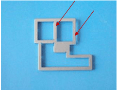
It’s critical to not only have a sound design that manages interference in theory but a manufacturable one that actually works in the real world. This means it’s vital to achieve specs and tolerances. Things like flatness, profile tolerance, corner angles, and clean edges contribute to the quality and performance of the finished shield. This is an area a precision stamper can help with by suggesting ways to optimize your design for efficient and cost-effective manufacturing. For example, the dimensions of the frame of this shield component were altered to be sturdier without compromising the overall SE of the finished product.
Metals for shielding, characteristics, and material choice
Metal shields are commonly made of copper, brass, nickel, silver, steel, or tin. The choice of materials involves balancing characteristics of the metals (e.g. conductivity, solderability, permeability, thickness, weight) to create the best protective shield within time and budget constraints. This is something an experienced precision stamper can provide advice about for custom EMI shields.
It also matters if the shield will be used to reflect radiation away from the circuit inside or to absorb radiation produced by it. A material’s ability to reflect depends on the wave’s impedance (i.e. how much it opposes the flow of the current) versus that of the shield material. In general, the grater the difference between the two, the more reflection and protection from outside radiation. The smaller the difference, the better a material is at absorbing and containing radiation.
Broadly speaking, for material selection:
Electrically dominant incident waves have high impedance and lower conductivity and reflect better. They are best countered by reflection with highly conductive metals, such as copper, silver, or brass.
Magnetically dominant incident waves have low impedance and higher conductivity so they are best countered by absorption/suppression of radiation with materials with lower conductivity, such as high permeability steel or stainless steel.
Another consideration in material choice is a phenomenon called “skin effect.” Circuits use either direct current (DC) or alternating current (AC) as a power source, but only alternating currents are impacted by skin effect. These currents tend to crowd into the top layers of a conductor, closest to the surface, increasing current density in that area of the material. This, in turn, increases the impedance of the current and lowers the conductivity of the conductor material. The higher the frequency the more pronounced the effect and the greater reduction in the ability of the material to absorb radiation.
How cleanliness and packaging affect EMI shields
So much time, work, and money goes into developing and producing custom EMI shields that are designed for a specific application, and they must be in the best condition possible when they reach the point of assembly. Your stamper should be able to provide carefully packaged finished parts that are not only free from defects but clean to your specifications so they stay that way.
The technical cleanliness of a shield, that is the number and type of particles (i.e. dust, fibers, metal fragments) or traces of oils on a part, affects many things from its solderability onto a PCB to potential short circuits due to stray metal particles.
While most parts are cleaned with one of several methods during manufacturing, part design can also influence levels of contamination in the first place. For example, the number and style of cuts on a part is directly related to the amount and size of stray particles that result from stamping. Edges shaped like a castle’s battlements, with several sharp corners, create more burrs and “chips” than a curved, wave-shaped edge. Making clean cuts with well-maintained tooling is another way to promote technical cleanliness while reducing time and costs associated with cleaning processes.
As we’ve noted above, the EMI/RFI shielding market is only going to grow as product developers add electronic and “smart” applications to more and more products and devices. That growth will be compounded by expanding offerings of self-driving and semi-autonomous vehicles in the coming years. As an OEM or supplier, it’s critical that you find a precision stamper that’s a true partner in manufacturing high-quality custom EMI shielding components that keep electronics protected and working properly. From DFM advice through cleaning and packaging for safe transport, experience and knowledge matter. Contact us to see the CEP Technologies difference.