Skip To Content

The 5G Network Brings Challenges for Designers and Precision Stampers

September 17, 2020


Most of us have heard of 5G and know it’s on the horizon. 5G refers to the fifth generation of network connectivity between devices. We commonly think about cell phones in this context but it includes any object (e.g. computer, car, appliance) connected to the Internet of Things (IoT) that can transmit and receive data. The exact timeline for its arrival is unclear, but there is definitely forward momentum. For example, “the share of 5G-connected cars that are actively connected to a 5G service will grow from 15% in 2020 to 74% in 2023, reaching 94% in 2028,” according to Gartner .

What will 5G look like when it arrives, and what does it mean for precision stamping? Read on.

What are some 5G use cases?

The two advantages of 5G connectivity are extremely high data transmission speeds and low latency (think of latency like human reaction time to new information). This means more data can be sent and received in less time. It also means devices will be able to take action based on received signals faster, almost in real time.

This speed and reliability brings many opportunities for communications between devices that are part of the network, such as:

  • Vehicle-to-everything (V2X) applications
    • Cars that can pick up signals from 5G-enabled DOT or weather stations about travel conditions
    • Vehicles that transmit signals to other nearby vehicles if they get too close
    • Location tracking devices
  • Healthcare applications
    • Medical devices to monitor health markers such as pulse or blood pressure
    • Remote robotic surgery
    • Transmitting large files of medical or technical data quickly
  • Augmented and virtual reality applications for industry
    • Wearable devices for equipment operators or maintenance workers that overlay the view with a diagram or instructions
    • Enhanced controls and monitoring for drone equipment for inspecting large equipment in mines, factories, etc.
    • Fabrication equipment that can communicate back and forth and make on-the-fly adjustments

The challenge for design and stamping

What sets this new generation of network connectivity apart is that it encompasses millimeter wavelengths, which are what enable the speeds and latency times for all of the use cases predicted and more. Millimeter wavelengths are fast but also very short with a small amplitude and they don’t travel as far as the microwaves used in 4G and older networks.

That means in order to fully realize the theoretical capabilities of 5G, designers and manufacturers need to address new limits of component size, cavity resonance, EMI/RFI interference, and heat management required to work with millimeter wavelengths and their effects. All of this must be balanced to create devices that function and interact correctly, especially when human safety is involved.

“5G networks will raise the technical standards of printed circuit board suppliers, electronics design companies and contract electronics manufacturers to achieve the higher frequencies and densities, faster speeds, understanding of advanced materials and their adoption required by 5G networks”, says EEWeb. In practice, as wavelengths get shorter, tolerances for components like shields, antennas, and even PCB traces become tighter.

For precision stampers, the challenges are:

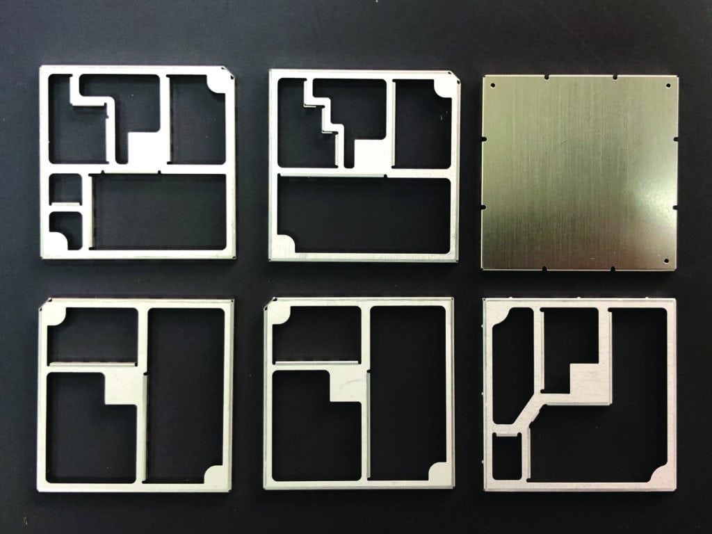
  • More EMI/RFI shields on circuit boards due to more components than in the past 
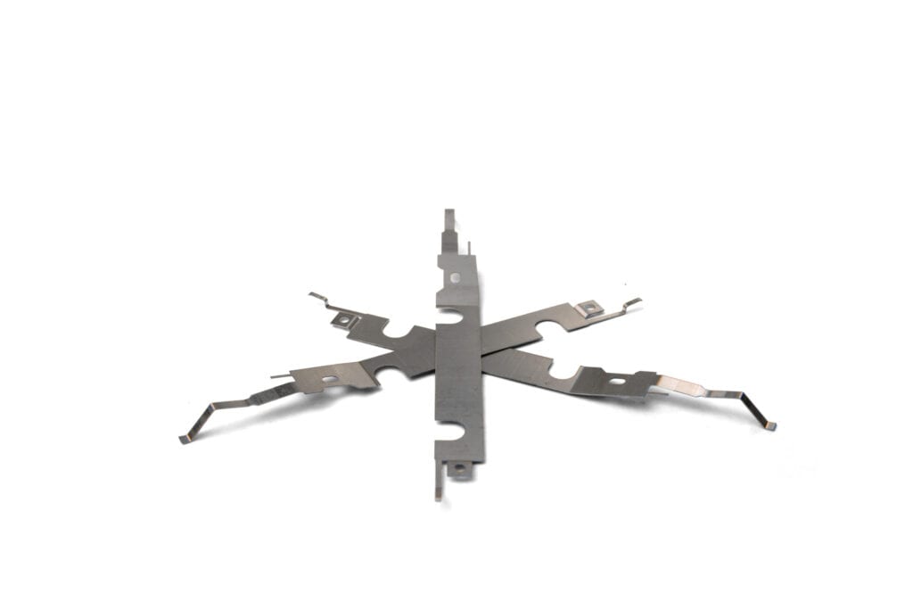
  • New components like tiny antennas and brackets
  • Small yet effective heat sinks that fit precisely at the point of greatest need
  • Smaller and more intricate stampings from the same materials already in use
  • Close attention to design-for-manufacturability (DFM)
  • Critical levels of technical cleanliness
    • Removing trapped fibers and particles
    • Removing stamping oils and lubricants that affect solderability
  • Careful tape and reel packaging to maintain cleanliness levels prior to end-use

The ability to create parts to customer requirements in the timeframe needed are top priorities in precision stamping. Always ask if your supplier has the experience and capacity to meet your needs when selecting stamping vendor. CEP can help – please contact us to learn more about our capabilities and set your next project in motion today.


Leave a Reply

Your email address will not be published. Required fields are marked *